This page contains some more detailed information about the baseband hardware and software.
- ESP32 sourcecode related:
- Changed from using INCBIN (which sucks) to using an include file for the FPGA image. Same functionality, less hassle.
- Added instructions in the project file, on building the code using the Arduino environment
- Some minor code fixes/cleanup
- Link to the ESP32 sourcecode providing all the info you need to compile the latest version
Digital processing
The baseband has inputs for composite video and stereo audio. Output is the ‘baseband’ signal, consisting of video, Nicam and FM carriers.
Almost all processing is done in the digital domain. The block diagram below shows the digital processing (only one FM channel shown).
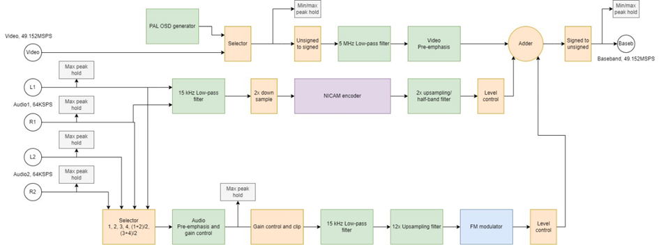
The analog video is low pass filtered by an analog anti-aliasing filter, then sampled at 49.152MHz using a 10-bit ADC.
First step in the digital domain is filtering by a steep low-pass filter. This filter removes all components above 5 MHz, which would interfere with the audio subcarriers. Then preemphasis is applied to the video, according to Rec. ITU-R F.405-1. Coefficients are programmable to select PAL, NTSC, SECAM or ‘FLAT’ (no preemphasis). Adjusting the coefficients also allows for video gain and polarity control.
Audio is low-pass filtered and sampled at 64 kHz with two 20-bit stereo ADCs. The digital audio is low pass filtered with a very steep filter at 15 kHz, as this is the maximum allowed frequency for both Nicam and FM. The filtered signal is applied to the Nicam encoder. The output of the Nicam encoder is a modulated carrier at an adjustable frequency, normally 5.85 or 6.552 MHz. As the Nicam encoder runs at half the output sample rate, the output is upsampled to the DAC rate of 49.152 MHz. After the upsampler, a level control block is placed to adjust the carrier level.
Four FM modulators are available, all consisting of an audio preemphasis, a gain/clip stage to control the modulation bandwidth and a FM/AM* modulator. The modulator input can be connected to any audio source. The preemphasis can be programmed for 50us, 75us, J17 and ‘flat’ (no preemphasis). The gain/clip stage limits the deviation to 50, 75, 100 or 125 kHz, resulting in FM modulation bandwidths of 130, 180, 230 or 280 kHz respective. The carrier frequency of the modulator is adjustable between 0 and 24.576 MHz and the level can be adjusted, as with the Nicam carrier.
The modulated FM/AM and Nicam carriers are added to the processed video to produce the complete baseband signal. A 12-bit DAC, followed by an anti-aliasing low-pass filter, converts the digital signal back to the analog domain.
To provide for precise readout of video and audio levels, several peak hold modules are available. For video and baseband, both the minimum and maximum values are stored; for audio, the maximum (absolute) values are stored, both before and after the preemphasis.
*only the first two modulators can do AM.
Control
All digital processing is done using modules implemented in programmable logic. These modules are controlled by a microcontroller which in itself is also implemented in programmable logic, a so-called ‘soft core’. The controller used is a Microblaze, a 32-bit CPU with 32kB of RAM, running at the 49.152 MHz clock.
This controller is responsible for controlling the modules in the processing pipeline. It is has access to an EEPROM and to the flash memory chip containing the FPGA firmware. The EEPROM is used to store the last used settings and can store up to 31 additional configurations (presets). The active configuration can be copied to and from these preset memories.
The microcontroller also provides different means to access the baseband. The main interface is i2c, via an i2c slave implemented in programmable logic. Besides that, it also reads two pushbuttons. Combined with the OSD, this gives a very basic means to set up the baseband without other hardware/software.
After power up, the FPGA initializes and the Microblaze booting process starts. Upon boot, the microcontroller reads the last used settings from EEPROM and uses these to initialize the registers of the various blocks. Then it enters its main loop, in which various tasks are handled, such as i2c transfers, button presses, reading video and audio levels, updating the OSD, et cetera.
I2c interface
The baseband board is controlled using i2c. The baseband acts as an i2c slave, capable of communicating in Fast-mode Plus (up to 1000 kHz). The slave is implemented using an i2c slave core and a Microblaze soft-core microcontroller.
The i2c bus allows access to all settings, the actual audio/video input levels, the actual baseband output level and the EEPROM (used to store setting presets). It is also possible to upgrade (and completely destroy) the firmware.
Usually, the baseband is controlled using the display board.
However, you can also control the baseband from any i2c master. On https://github.com/pe1obw/baseband_config you’ll find a Python project to control the baseband from a PC using a relatively cheap (15 euro at amazon.nl) USB <-> i2c interface. Note that this tool is meant as a starting point; not much testing has been done so far :-).
The slave uses clock stretching to allow the microcontroller to read or write new data from/to the peripheral. Make sure the master supports this correctly! For some reason, clock stretching seems to be difficult black magic for many manufacturers and programmers…
Baseband control protocol
Here’s some starting information for those who want to do it their selves.
The i2c slave address is 0xB0.
For most actions, the baseband is addresses as a memory mapped device. To write data to the baseband, use the following sequence:
<start> <slaveaddr> <addr_hi> <addr_low> <data> … <stop>
To read data from baseband:
<start> <slaveaddr> <addr_hi> <addr_low> <start> <slaveaddr|1> <read(ACK)> … <read(NAK)> <stop>
The <addr_hi> and <addr_lo> make up a 16-bit address. The address space is divided in multiple sections, listed in table ‘Baseband address space‘ below. When reading or writing, the address is incremented automatically.
Memory mapped regions
The internal structures for OSD memory, font memory, settings and more are directly byte-accessible via i2c. For example, the i2c interface gives direct access to the internal settings. The baseband has its settings stored in internal memory as a C-struct, see the C header files for the details. The bytes in the C structure can be accessed directly. The first byte of the struct can be read from address 0x1000.
Commands
Address range 0x3xxx is preserved for ‘Commands’. These work slightly different. To issue a command, write the command address followed by a single byte as parameter, which is always > 0. For commands without a parameter (such as ‘I2C_ACCESS_COMMAND_UPDATE_SETTINGS’), this field should be ‘1’.
Commands are executed in the background, as most of them take a considerable amount of time to complete. During their execution, the i2c bus can be used for other transfers, such as VU meter readout.
The execution status of the pending command(s) can be read to see if the command has completed. To read the status of a command, issue the address (without parameter) and read back the status byte. The command is completed when the status equals zero.
Note that issuing the same command again while it is still in progress has no effect.
Example: modify settings
First, get a full copy of the settings by reading sizeof(SETTINGS) bytes from address 0x1000 into a local copy of a SETTINGS struct:
<start><0xB0><0x10><0x00><repeated_start><0xB1><byte0><byte1>....<byte n><stop>
where byte 0…byte n are the bytes of the baseband’s internal settings struct.
Then display, store and/or modify your local settings. To write back the local copy to the baseband, do a write to address 0x1000:
<start><0xB0><0x10><0x00><byte0><byte1>...<byte n><stop>
The settings are now copied to the baseband, but have no effect yet. To activate the new settings, give the command I2C_ACCESS_COMMAND_UPDATE_SETTINGS:
<start><0xB0><0x30><0x00><0x01><stop>
When desired, you can read back the status of the command execution to see if it’s completed:
<start><0xB0><0x30><0x00><repeated_start><0xB1><status>
When completed, the new settings are active.
| I2C_ACCESS_DISPLAY | 0x0000 – 0x03FF | R/W, maps to display memory, 40 columns x 16 rows = 640 bytes |
| I2C_ACCESS_FONT_MEMORY | 0x0400 – 0x07FF | R/W, maps to font memory, 128 characters, each 8×16 pixels = 2048 bytes |
| I2C_ACCESS_SETTINGS | 0x1000 – 0x1FFF | R/W, maps to SETTINGS |
| I2C_ACCESS_READOUT | 0x2000 – 0x2FFF | RO maps to HW_INPUTS |
| I2C_ACCESS_COMMAND | 0x3000 – 0x3FFF | R/W maps to commands, read gives status (0=done), no auto address increment! |
| I2C_ACCESS_VIEW_SETTINGS | 0x4000 – 0x4FFF | RO maps to SETTINGS preview (= the result from COMMAND_VIEW_PRESET) |
| I2C_ACCESS_READ_PRESET_STATUS | 0x5000 – 0x5FFF | RO maps to PRESET_FLAGS, 32 bits (4 bytes), bit=1 indicates if a preset is used |
| I2C_ACCESS_INFO | 0x6000 – 0x6FFF | RO maps to INFO |
| I2C_ACCESS_FLASH | 0x7000 | R/W maps to flash SPI interface, see description in file header |
// Commands. To execute, write a byte (> 0) to the address. To retrieve status, read from this address
#define I2C_ACCESS_COMMAND_UPDATE_SETTINGS	0x3000		// <1>   	   Update hardware registers (activate settings)
#define I2C_ACCESS_COMMAND_READ_PRESET		0x3001		// <preset nr> Read config from preset 1..31 and activate it
#define I2C_ACCESS_COMMAND_STORE_PRESET		0x3002		// <preset nr> Store current config in preset 1..31
#define I2C_ACCESS_COMMAND_ERASE_PRESET		0x3003		// <preset nr> Erase current config in preset 1..31
#define I2C_ACCESS_COMMAND_VIEW_PRESET		0x3004		// <preset nr> Read config from preset 1..31 and copy to 'preview' settings
#define I2C_ACCESS_COMMAND_REBOOT           0x3005		// <1> 		   Reboot FPGA board after 500ms delay